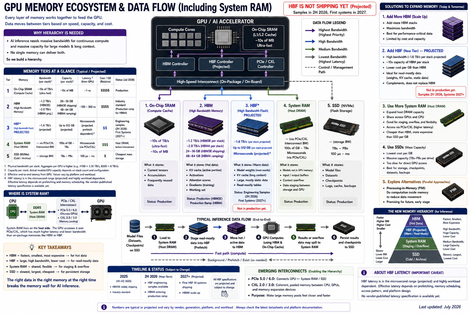
How data actually moves through an AI server, why HBM became the industry’s tightest bottleneck, and where projected technologies like High Bandwidth Flash and CXL fit into the picture.
The diagram shows the typical staged path. On systems configured with GPUDirect Storage, NVMe drives can DMA data directly into HBM, bypassing the System RAM hop.
The common mental model of AI hardware goes something like this: a GPU loads the model into its memory, then starts computing. Simple. It is also wrong in almost every detail that matters.
A modern AI server contains an entire hierarchy of memory technologies, each engineered for a different balance of speed, capacity, and cost. Some of these memories respond in billionths of a second and cost so much per gigabyte that they are measured out in megabytes. Others store petabytes cheaply but respond thousands of times more slowly. None of them can do the whole job alone.
Understanding how these layers cooperate explains a lot of things that otherwise look mysterious: why data-center GPUs carry six-figure price tags, why high-bandwidth memory has become the single tightest constraint in AI infrastructure, and why NVIDIA, AMD, Samsung, Micron, SK hynix, and SanDisk are all pouring billions into memory technologies most people have never heard of.
Here is the hierarchy at a glance, fastest and smallest at the top. Each tier is unpacked below.
| Memory tier | Bandwidth | Typical capacity | Primary AI function |
|---|---|---|---|
| On-chip SRAM | Fastest in the system; nanosecond access | Kilobytes to megabytes | Tiles of data being computed right now |
| HBM3E / HBM4 | 1.2+ TB/s per stack; up to 8 TB/s per GPU shipping today | 36 GB per stack; up to 288 GB per GPU | Active model weights, activations, KV cache |
| HBF (projected) | Up to 1.6 TB/s read per stack (target) | Up to 512 GB per stack (target) | Read-mostly weights and long-context data |
| System RAM (DDR5 / LPDDR5X) | Tens of GB/s per channel; up to 1.2 TB/s in tightly coupled designs | Hundreds of GB to terabytes | Staging, overflow, KV-cache offload |
| CXL-pooled DRAM | Link-limited; slower than local DRAM | Terabytes, shared across hosts | Warm capacity: spilled caches, retrieval indexes |
| NVMe SSD | Roughly 14 GB/s per PCIe 5.0 drive | Terabytes to petabytes | Models at rest, checkpoints, datasets |
Picture a line cook during a dinner rush. The cook’s hands are the GPU cores. Whatever is being chopped right now sits on the cutting board. Ingredients for the next few dishes wait on the counter. The walk-in refrigerator holds everything needed for tonight’s service, and the dry-storage pantry in the back holds bulk supplies for the week.
No sane kitchen keeps the entire pantry on the cutting board. There isn’t room, and most of it isn’t needed this second. Instead, ingredients flow forward as they’re needed: pantry to walk-in, walk-in to counter, counter to board. Every step farther from the cook’s hands means more walking and more waiting.
Computers are organized the same way, for the same reason. Fast memory is expensive and physically small; large memory is cheap and slow. So instead of one giant pool, an AI server arranges its data in layers, and the whole engineering game is keeping the GPU’s “cutting board” stocked so those absurdly expensive cores never sit idle.
The fastest memory in the system lives on the GPU die itself: registers, L1 cache and shared memory inside each streaming multiprocessor, and a larger L2 cache shared across the chip. This is SRAM, and it responds in nanoseconds. It is also tiny. Where HBM is measured in gigabytes and SSDs in terabytes, on-chip SRAM is measured in kilobytes and megabytes, because each SRAM cell needs six transistors and eats die area that could otherwise hold compute units.
That scarcity shapes how AI software is written. Techniques like FlashAttention exist precisely to restructure attention math so intermediate results stay in on-chip SRAM instead of making round trips to HBM. When a kernel is tuned well, data gets reused many times per visit to the chip. When it’s tuned badly, the GPU spends its life waiting.
High Bandwidth Memory is what people usually mean when they talk about a data-center GPU’s memory capacity. It is DRAM, but packaged in a way ordinary DRAM never is: multiple dies stacked vertically, connected through the stack by thousands of vertical channels called through-silicon vias (TSVs), and mounted millimeters from the GPU die on a slice of silicon called an interposer.
That short, extremely wide connection is the entire point. A conventional DDR5 module talks to a CPU over a 64-bit channel; an HBM3E stack talks to a GPU over a 1,024-bit interface. Current 12-high HBM3E stacks hold 36 GB and deliver more than 1.2 TB/s of bandwidth per stack. Put eight of those around a GPU and the numbers get large fast: NVIDIA’s Blackwell Ultra (B300) carries 288 GB of HBM3E at 8 TB/s of aggregate bandwidth.
The next step is already defined. JEDEC published the HBM4 standard (JESD270-4) in April 2025, doubling the interface to 2,048 bits and supporting up to 2 TB/s per stack. SK hynix has already completed HBM4 development and readied mass production, with parts that run faster than the baseline spec. NVIDIA’s Rubin GPU, sampling in late 2026, pairs 288 GB of HBM4 with up to 22 TB/s of aggregate memory bandwidth.